
Распиновка, расположение выводов и внешний вид последовательного интерфейса:
EIA530 (RS530)
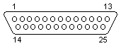 (at the DTE)
 (at the DCE)
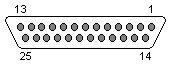
CORRECT?
25 PIN D-SUB MALE at the DTE (Computer).
25 PIN D-SUB FEMALE at the DCE (Modem).
PinNameDirDescriptionCircuitPaired with
1

Shield
18
2
TxD

Transmitted Data
BA
14
3
RxD

Received Data
BB
16
4
RTS

Request To Send
CA
19
5
CTS

Clear To Send
CB
13
6
DSR

Data Set Ready
CC
22
7
SGND

Signal Ground
Ground
21
8
DCD

Data Carrier Detect
CF
10
9

Rtrn Receive Sig. Elmnt Timing
DD
17
10

Rtrn DCD
CF
8
11

Rtrn Transmit Sig. Elmnt Timing
DA
24
12

Rtrn Transmit Sig. Elmnt Timing
DB
15
13

Rtrn CTS
CB
5
14

Rtrn TxD
BA
2
15

Transmit Signal Element Timing
DB
12
16

Rtrn RxD
BB
3
17

Receive Signal Element Timing
DD
9
18
LL

Local Loopback
LL
1
19

Rtrn RTS
CA
4
20
DTR

Data Terminal Ready
CD
23
21
RL

Remote Loopback
RL
7
22

Rtrn DSR
CC
6
23

Rtrn DTR
CD
20
24

Transmit Signal Element timing
DA
11
25

Test Mode
TM
Note: Direction is DTE (Computer) relative DCE (Modem).
Contributor:
Joakim Цgren, Greg A. Woods
Source:
RS530 Page made-it.com/CKP/rs530.html at Connectivity Knowledge Platform (Made IT)
Copyright © The Hardware Book Team 1996-2004.
May be copied and redistributed, partially or in whole, as appropriate.
Document last modified: 2002-01-13